Difference between revisions of "POT4a"
From DIDEAS Wiki
m |
m |
||
| Line 25: | Line 25: | ||
[[image:Rpot4a-pcb-top-reva-061605.png|right|thumb|80px|top side]] | [[image:Rpot4a-pcb-top-reva-061605.png|right|thumb|80px|top side]] | ||
[[image:Rpot4a-pcb-bot-reva-061605.png|right|thumb|80px|bottom side]] | [[image:Rpot4a-pcb-bot-reva-061605.png|right|thumb|80px|bottom side]] | ||
| + | |||
| + | |||
*POT4a is a green PCB with white silk screen on two sides. | *POT4a is a green PCB with white silk screen on two sides. | ||
| Line 39: | Line 41: | ||
*SN1 : Vref=9.79V, CB1,CB3=2.2uF, CD1=1uF has LP2 and dX/dt; not populated adjustable gain; additional CB caps could be populated | *SN1 : Vref=9.79V, CB1,CB3=2.2uF, CD1=1uF has LP2 and dX/dt; not populated adjustable gain; additional CB caps could be populated | ||
| + | ==Frequency Response== | ||
| + | [[image:Pot4 derivative freq res.png|240px]] | ||
==Design Files== | ==Design Files== | ||
*[[Media:Pot4a-sch-reva-062205.pdf]] | *[[Media:Pot4a-sch-reva-062205.pdf]] | ||
Revision as of 06:39, 13 July 2005
Contents
Revisions from POT4
- add 5pin, 1.25mm header for strain gauge
- removed unused input resistors and capacitors
- On POT4 a 1meg resistor was stacked on CC3 - this resistor added to SCH and PCB
- removed 4th order filter, changed 3way jumper to 2way
- 2nd order filter is now NON-Inverting
- input cable shield can be connected to COM via 0603 resistor
- changed PCB pattern for output driver caps to CAP200-SQ (accurately represents component shape)
- changed 0805 output cable CAP to 1206. Panasonic X5R series @ 25V 1uf to 10uF!
- added 10 turn POT for variable gain (optional)
- changed CD2 (0.1u in derivative circuit) to 1206 size (was 0805)
Power Supply
- +12V, GND, -12V recommend
- Supply current < 50mA (20mA typical)
- Maximum supply voltage is +-15V
Identification
- POT4a is a green PCB with white silk screen on two sides.
- Dimensions 1.75" x 0.85"
- Two mounting holes (diameter = 0.125"), top side clearance > 0.25"
- The color of DL1,DL2 indicates the input configuration of the board
Led Indicators
- (DL1, DL2) : A pair of single LEDs indicate the present of power. These LEDs are aligned with the power input to the boards.
- DK1 : The intensity of this dual RED/GREEN LED indicates the voltage of the "position signal".
Assembly Notes
- SN1 : Vref=9.79V, CB1,CB3=2.2uF, CD1=1uF has LP2 and dX/dt; not populated adjustable gain; additional CB caps could be populated
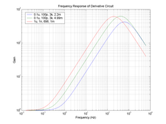
Frequency Response
Design Files
- Media:Pot4a-sch-reva-062205.pdf
- Media:Rpot4a-pcb-top-reva-061605.pdf
- Media:Rpot4a-pcb-bot-reva-061605.pdf
- Gerber files and Tango DOS source (6-16-05)


